Dr. Ki and His Chemistry Students Developing Semiconductors Using Sunlight and Water As Renewable Energy Source

Summer 2018 Issue
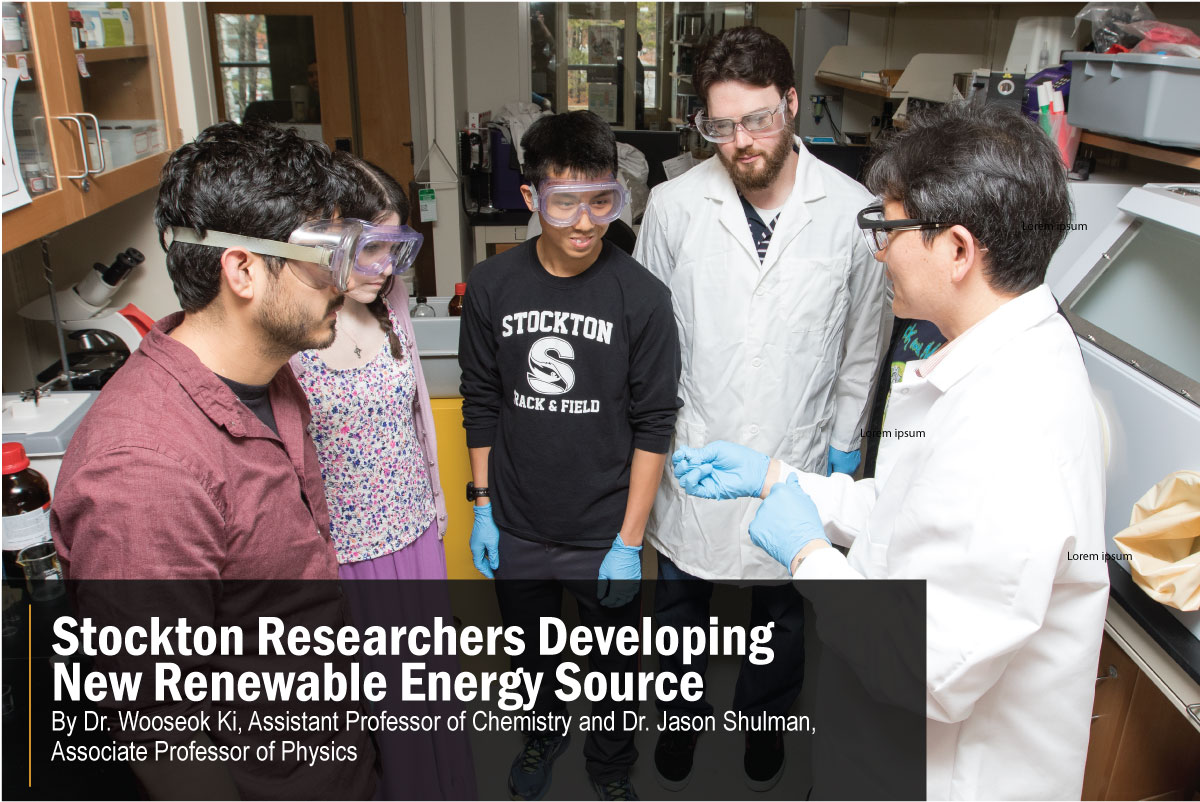
Dr. Wooseok Ki, Assistant Professor of Chemistry (far right), speaks with Dr. Jason
Shulman, Associate Professor of Physics, and researchers (left to right) Anthony Bautista,
Chemistry '18, Anastasia (Nastya) Morozova, Chemistry major, and Daniel Do, Biochemistry
major in the Chemistry research laboratory. (Photo credit: Susan Allen)
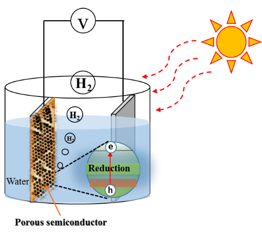
FIgure 1. A schematic diagram of hydrogen production using porous semiconductor by sunlight
There is an increasing demand for harvesting renewable and sustainable energy sources due to an accelerating global energy consumption. International Energy Outlook projected that renewables are expected to be fast-growing energy sources, increasing by an average of 2.3 percent per year between 2015 and 2040.[1] Hydrogen is an ideal renewable energy source that can be stored, is transportable, and can be converted to electricity using fuel cells in a clean manner, without producing CO2.[2] A key challenge, however, is to produce cost-effective and environmentally friendly renewable hydrogen on a large scale. Recently, sun-driven water splitting semiconductor materials (also known as photocatalysts) have drawn considerable attention because they require only sunlight and water as sustainable resources to produce hydrogen: semiconductor materials absorb energy from sunlight and facilitate the breakdown of water to hydrogen and oxygen as seen in Figure 1. Therefore, producing efficient, cost-effective water splitting semiconductors is the key to the advancement of solar-hydrogen production on a large scale. To do so, Dr. Wooesok Ki has initiated an exciting research project to develop simple, solution processable, template-assisted microporous semiconductor materials to improve water-splitting performance. One of the most critical steps in the construction of such semiconductors is to create a uniform monolayer of polystyrene microspheres (500 nanometers in size, roughly 200 times thinner than a human hair) on substrates.
Figure 2 shows a 6 µm x 6 µm Atomic Force Microscope (Stockton's new AFM used in collaboration with Dr. Jason Shulman) image of a monolayer produced by students in Ki’s research group. In the parlance of crystallography, the spheres have been arranged in a close-packed hexagonal lattice. Interestingly, we have observed defects that are found in atomic crystals, most commonly grain boundaries and vacancies. These defects can be observed in Figures 3 and 4.
Hydrogen is an ideal renewable energy source that can be stored, is transportable, and can be converted to electricity using fuel cells in a clean manner, without producing CO2.[2]
Ultimately, our goal is to create nanoporous WS2 and MoS2 semiconductors by pouring molecular precursor solution into the template of a close-packed monolayer of polystyrene microspheres. Thermal processing will remove polystyrene microspheres, resulting in the formation of a two dimensional, ordered nanoporous structured semiconductor. Finally, the nanoporous MoS2 and WS2 semiconductor materials will be tested for efficiency of hydrogen evolution in collaboration with Rutgers University researchers.
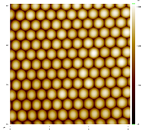
Figure 2. A 6 µm × 6 µm AFM image of 500 nm spheres arranged in a close packed structure.
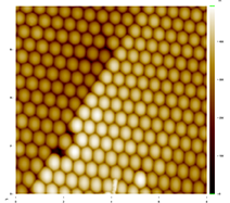
Figure 3. A grain boundary. Two orientations of crystals cannot meet perfectly. This defect is likely due to a single sphere filling the space of two (lower left). The scale is 8 µm × 8µm
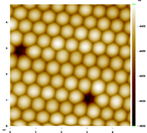
Figure 4. Vacancies were also observed. The scale is 5 µm ×5 µm.